Stretchable Electronics Twist and Strain
January 23, 2009

miami
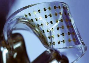
Optical image of a freely deformed stretchable array of complementary metal-oxide semiconductor inverters. Image Credit: John A. Rogers, University of Illinois at Urbana-Champaign.
An intercollegiate research project has resulted in the development of materials and mechanical design strategies for flexible electronics suited for use in biomedical devices, among other applications. Because conventional wafer-based technologies can no longer satisfy some needs of developing devices, the researchers endeavored to explore electronic systems that could undergo extreme strain and bending without a reduction in electronic function.Dubbing its design strategy noncoplanar mesh design, the team began by fabricating active circuits on silicon islands that form a chemically bonded prestrained elastomeric substrate. Upon releasing the prestrain, the circuits' interconnects buckle and bend, creating arc-like formations that enable flexibility without compromising electrical properties. Single crystalline silicon nanomaterials served as the foundation of the design. Employment of these nanomaterials for the semiconductor demonstrated flexibility in CMOS integrated circuits close to that of similar devices that were formed on wafers. The team, consisting of professors at the University of Miami College of Engineering, the University of Illinois, and Northwestern University, detailed their findings in the December issue of the Proceedings of the National Academy of Sciences.
You May Also Like


