
Sign up for the QMED & MD+DI Daily newsletter.
Miniaturized Cutting and Drilling Using Picosecond Lasers
Bob Michaels
July 1, 2014
9 Min Read
.svg?width=850&auto=webp&quality=95&format=jpg&disable=upscale "Miniaturized Cutting and Drilling Using Picosecond Lasers")
Offering precision, high throughput, and cost savings, picosecond laser processing is suitable for fabricating microfluidic technologies, miniaturized implants, drug-delivery catheters, and other devices.
By Dirk Müller, Coherent Inc.
Traditionally, electrical discharge machining (EDM) or conventional laser tools have been used to manufacture a range of precision medical devices. However, these manufacturing methods cannot be used to achieve the miniature features, precision, surface quality, and yields required for manufacturing microfluidic devices for clinical lab-on-a-chip applications, precision drug-delivery catheters, next-generation ophthalmic blades, and a host of miniaturized implants. To manufacture such devices, alternative high-precision micromachining methods are required. This article examines the use of the picosecond laser to perform micromachining processes in medical device manufacturing applications.
Making Microfluidic Devices
Microfluidics is a broad field that encompasses medical and clinical lab devices and applications. In addition to lowering costs, microfluidic devices enable miniaturization, automation, and parallel processing in lab-on-a-chip devices, supporting the growing demand for personalized medicine. Representing a massive growth opportunity for the medical device industry, the sector is forecast to grow beyond $5 billion before the end of the decade.
|
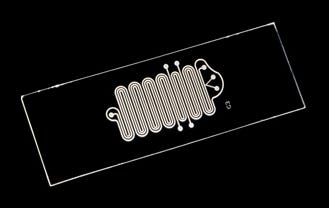
Figure 1. Picosecond lasers provide a flexible and versatile method of creating complex grooves, holes, and wells in various materials, including in glass microscope slides. |
Relying on surface tension and other parameters, microfluidic devices contain, mix, or transport fluids through channels and holes at the submicron scale, as shown in Figure 1. They frequently incorporate a three-dimensional pattern of channels, which are typically created by machining two or more plastic or glass layers that are laminated together using a thermal frit, laser weld, or other bonding process.
The assembled device can be used in such emerging applications as patient genome sequencing and cancer genotyping applications, ultimately promising to miniaturize several existing macroscopic medical analysis methods. A primary benefit of microfluidic technology is that it can perform complex analysis and testing on minute amounts of blood and other fluids down to 0.001 ml. Microfluidics also encompasses catheter technologies and drug-release tools based on inkjet-type technology. In such applications, the use of holes with diameters as small as 20 µm enables automated drug delivery with unprecedented dosing capability and temporal precision.
Picosecond Laser Processing
A relatively new type of laser that is already used to produce such products as touch screens and solar cells, industrial picosecond lasers are capable of delivering the performance, speed, and economy required to fabricate microfluidic and other miniaturized medical devices. Picosecond lasers can create high-precision holes, channels, and marks on such materials as glass, silicon, and polymer without producing edge damage or debris. These simple features, in turn, become the building blocks for creating a variety of microfluidic devices.
|
Figure 2. By removing material partially through photoablation, picosecond lasers produce higher-quality holes than traditional laser techniques. |
In contrast, current tools cannot achieve the micron-level precision requirements of microfluidic devices. For example, mechanical drills cannot produce the hole sizes required in microfluidic applications. Even at the larger end of the microfluidic range, tool wear and breakages make economical, consistent, high-throughput manufacturing impossible using mechanical methods.
EDM is a potential option for drilling simple holes in the few microfluidic devices based on metal. However, EDM electrodes wear with use, impacting product consistency and resulting in frequent replacement downtime. Moreover, EDM typically produces inferior hole quality, resulting in rough side walls.
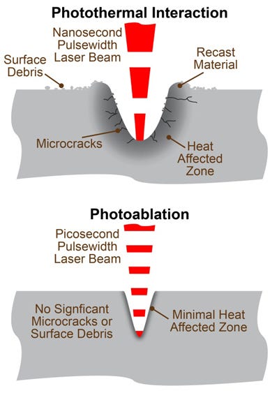
While traditional pulsed lasers have long been employed in medical device manufacturing applications to produce micron-scale holes and other features, they have pulse widths in the tens of nanoseconds range. Nanosecond pulses remove material using a thermal process in which surface material is boiled and ejected as melted and vaporized material. As a result, most common pulsed laser sources also produce a heat-affected zone (HAZ), which results in thermal damage or microcracks.
Picosecond pulses, in contrast, are more than a thousand times shorter than nanosecond pulses, generating significantly higher peak power in the megawatt range. As illustrated in Figure 2, higher peak power triggers a cold photoablation process, in which a higher proportion of material is removed in a vaporized state. This process reduces HAZ and largely eliminates such defects as burrs on hole edges, recast material, and surface debris, as shown in Figure 3. Thus, picosecond laser processing is particularly suitable for drilling holes in such thermally sensitive materials as glass and polymers.
|
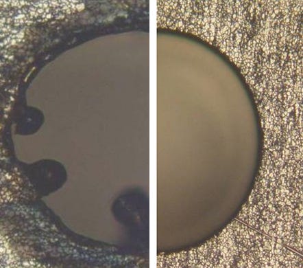
Figure 3. A 200-µm-diameter hole drilled in stainless steel using a picosecond laser (right) reveals cleaner results than a 200-µm-diameter hole drilled using a nanosecond laser (left). |
While the processing advantages associated with picosecond lasers have long been known in the R&D lab, the recent advent of compact, robust picosecond lasers is enabling their emergence in cost-conscious volume manufacturing environments. For example, the Talisker and Rapid series of picosecond lasers from Santa Clara, CA-based Coherent Inc. feature laser head dimensions as small as 180 × 330 × 460 mm, simplifying integration into production lines and workstations. Available with a choice of infrared, visible, or ultraviolet outputs, they can machine most materials employing a wavelength that is optimally absorbed by the target, maximizing process efficiency and eliminating the potential for peripheral thermal effects. Their high power can achieve material ablation rates up to 1.5 mm3/sec.
Medical devices featuring complex machined patterns and shapes must often undergo advanced micromachining, requiring communication between the laser and the motion control system. Using picosecond laser systems, communication can be achieved using real-time control of pulse energy, pulse repetition rate, and pulse timing. When machining films, for example, the control of these parameters enables users to maintain a finite cut depth around sharp corners and ends, although the motion control system may not always deliver constant velocity. This control also allows machinists to avoid overshooting cuts onto background webbing or other support substrates.
Machining Medical Device Materials
While the deployment of picosecond lasers in the medical device manufacturing industry is still in its infancy, several materials have already been qualified for use with this technology, including nitinol, cobalt chrome, heat-sensitive polymers, and borosilicate glass.
|
Figure 4. A microfluidic channel machined in FEP using a 355-nm picosecond laser. |
Machining Polymers. Several polymers exhibit a combination of biological inertness and mechanical properties, making them suitable for use in medical device applications. For example, microfluidic dispensing devices in catheter applications are often made from fluorinated ethylene propylene (FEP).
A strong absorber of ultraviolet light, FEP can be machined using any ultraviolet laser. However, because this material is sensitive to heat, processing micron-level features using traditional laser methods is impractical. Ultraviolet picosecond lasers, on the other hand, can cut, drill, and mark polymers using a maximum of processing energy with a minimum of unwanted heat. As shown in Figure 4, ultraviolet picosecond lasers can routinely drill hole diameters measuring less than 10 to 100 µm in FEP tubes, enabling catheters to deliver controlled dosage volumes.
Drilling Holes in Glass. The ability of picosecond laser pulses to achieve high peak power makes them suitable for cutting glass with clean edges, as illustrated in Figure 5. It also enables users to reverse-drill holes with aspect ratios as high as 100:1.
When lasers are used to drill small holes, the maximum aspect ratio is limited by the focusing properties of the beam. The smaller the hole, the tighter the required focus, which means a reduced depth of focus. As the focused laser is pushed farther into the hole, its entrance diameter increases. But the high peak power of picosecond lasers changes the optical properties of glass, causing an effect known as self-focusing. This effect can be exploited to drill glass by focusing through the glass onto the rear surface. The hole is then created as the focusing lens is backed away from the front surface. Based on this self-focusing effect, perfect tight focus is maintained throughout the drilling process, leading R&D groups to use this method to drill parallel-sided holes in 1-mm-thick glass with diameters as small as 10 µm. No other drilling method can match such high aspect ratios at such small diameters.
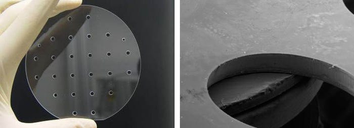
|
Figure 5. 3-mm-diameter (button) holes cut in a 5.5-mm-thick glass substrate. |
Laminates. Another benefit of picosecond lasers is their ability to mark composite or layered materials. When the surface layer is transparent to a laser wavelength, the underlying layer can be marked without compromising the surface layer. While this method is commonly used to mark consumer electronics with a branded logo, it can also be used to produce microfluidic component markings for product traceability, such as a bar code or QR code. The untouched clear coating ensures biological inertness to the marked material.
Picosecond lasers can also be used to machine laminates. For example, when a composite material consists of a stack of layers--each with different material properties--a picosecond laser can selectively remove layers to create a functional electronic circuit on a nonconducting substrate. Software flexibility enables the laser to produce lab-on-a-chip devices in which complex fluid channels and electrical interconnects can be rapidly prototyped and evolved during preclinical trials.
Conclusion
There is a fast-growing need in the medical device industry for versatile tools that can perform drilling, cutting, and other machining processes. Because its processing capabilities have already been demonstrated in other demanding markets, the picosecond laser is a good candidate for supporting medical device applications.
|
Dirk Müller is director of product line management at Coherent Inc. Before joining Coherent, he was director of marketing and sales at Lumera Laser and vice president of operations at Kapteyn-Murnane Laboratories. He also worked as a senior research scientist at Corning Inc., where he specialized in characterizing photonic bandgap fibers. During his professional career Müller has published articles in numerous journals, including Science, Nature, Physical Review Letters, Optics Letters, and Laser Focus World. Reach him at [email protected].
About the Author(s)
You May Also Like

.png?width=300&auto=webp&quality=80&disable=upscale)