Sign up for the QMED & MD+DI Daily newsletter.
When Laser Ablation of Parylene Makes Sense
Qmed Staff
August 15, 2014
10 Min Read
.svg?width=850&auto=webp&quality=95&format=jpg&disable=upscale "When Laser Ablation of Parylene Makes Sense")
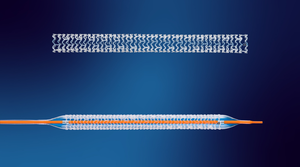
Laser ablation of parylene offers superior capability for designs where small features, precise alignment, and custom shapes are needed.
By David L. Wall, Resonetics LLC
Parylene is a conformal coating widely used in the medical device and microelectronics industries. It has many highly desirable characteristics: chemical resistance, biocompatibility, thermal stability, high dielectric strength, low friction, optical transparency, hydrophobicity, and low permeability to gases. It provides a pin-hole free, hermetic, homogeneous surface to protect underlying surfaces or components. Some products require a partial parylene coating, leaving certain surfaces or components uncovered. In these applications, conventional masking blocks the deposition of parylene on those surfaces directly shielded by the contact mask.
Masking is more challenging, however, as medical devices become smaller and more integrated in applications such as neuromodulation, neurovascular, electro-surgical and other microelectronic-based applications. For these more difficult applications laser ablation offers medical device designers unique capabilities such as higher precision, smaller feature sizes and adaptability to alternate geometries.
Parylene Technology
Parylene is a trade name for a family of polymers based on poly(p-xylene). The most basic member of the parylene family is parylene N, which is a linear polymer chain of multiple p-xylene monomer units. The other two most common type of parylene used in medical device and microelectronics applications are parylene C and parylene D, in which one or two chlorine atoms are attached to the phenyl ring. (See the image below.) There are many other flavors of parylene (AF-4, VT-4, X, AM, A, etc.) in which fluorine or other functional groups are incorporated in or onto the polymer chain for the purpose of tailoring specific properties.
|
Parylene types (Image courtesy of Resonetics) |
Parylene coating is a vapor deposition process in which a precursor compound is pyrolized to "crack" this compound into gaseous monomers. These monomers are then transmitted into a low pressure deposition chamber where they deposit and polymerize on the target component surface. The deposition process is performed at room temperature so there is no thermal stress to the target component. The parylene coating thickness is controlled by the deposition chamber conditions and deposition time.
By its nature, this vapor deposition process allows the parylene monomers to uniformly coat all surfaces, even into the smallest corners or crevasses, making it an ideal conformal coating for critical applications. This is a tremendous advantage over liquid spray or dip coating processes where surface tension and gravitational forces come into play, limiting uniformity of coverage.
Since parylene is coated on all exposed surface targets, parylene coating vendors have developed masking methods such as tape stickers (e.g. strips, dots, or other cut shapes) that are manually affixed to the surface, and liquid compounds (such as latex) that can be applied using automated dispensing systems. These masks, whether the sticker or dried compound, must be peeled off after the parylene coating is applied.
The main disadvantages of these masking methods include:
Higher cost: Masking and de-masking are labor intensive processes.
Less-than-acceptable quality: Masking leaves rough edges around the area where the parylene coating is torn during mask removal. Parylene can also "slip" under the mask and coat unwanted areas.
Design constraints: Engineers are constrained in their design choices because the results of masking methods do not precisely and accurately leave uncoated surfaces in the proper location, nor can the mask be fabricated with dimensions at the micron level. Also, the method is best suited for planar surfaces only.
Laser Ablation Technology
Laser ablation after the parylene coating process is an alternative to physical masking prior to the coating process is. Laser ablation is the mechanism of applying laser energy to a material surface and converting the material to a gas or plasma by one or more physical chemical mechanisms. Laser ablation typically utilizes pulsed laser sources, with each laser pulse removing a fraction of the material thickness.
The main advantages of laser ablation after the parylene-coated process are:
Lower cost: Especially for complex features such a row of tightly-spaced contact pads to take advantage of processing all at one time.
Better quality: Produce 100% parylene-free areas, especially with the photo-chemical ablation process.
No design compromise: Lasers can precisely control the area of ablation with dimensions as small as one micron. Lasers can also ablate true 3-D devices of varying heights.
The two main laser ablation mechanisms are photo-thermal ablation and photo-chemical ablation. In photo-thermal ablation, a thermal laser source such as an infrared CO2 laser delivers concentrated heat to the material, causing it to pyrolyze or to boil and evaporate, depending upon the thermal characteristics of the material. This is a rapid process, but in many cases, a thin layer of polymer may remain, requiring a secondary process to create a critically-clean substrate surface.
With photo-chemical ablation, the laser energy is delivered in the form of ultraviolet photons with much higher energy than IR thermal photons. These photons couple with the bonding electrons and once the photon energy is higher than the bond energy, the resulting bond-breaking fragments the polymer molecules. UV laser wavelengths below 266 nm couple very well with parylene to produce very clean surfaces at relatively low laser energy density without damage to the substrate. The table below shows bond energy for some of the primary chemical bonds in the parylene (assuming parylene C or D) as well as photon energies from several candidate laser sources.
Chemical bond | Bond Energy (eV) | Laser Type and Wavelength | Photon Energy (eV) |
C-C | 3.60 | Diode-pumped solid-state 266nm | 4.66 |
C-H | 4.28 | Excimer 248nm | 5.00 |
C-Cl | 4.12 | Excimer 193nm | 6.43 |
Parylene can also be ablated using newer generation ultrafast lasers--picosecond and femtosecond lasers. With these lasers, the ablation mechanism is associated with the ability to deliver a high peak power density to the material in an extremely short pulse. Since the pulse is so short, the time is insufficient for the laser energy to convert to thermal energy that can propagate into the substrate or surrounding material.
Achieving small feature size (as small as one micron) is one of the principal advantages of laser ablation. The ultimate size and precision are limited by the laser wavelength and the optics used to deliver the beam to the target surface. Laser ablation also offers other advantages compared conventional tape masking. Removal of the masking tape results in irregular torn edges of the parylene coating at the edges of the masked area. With laser ablation, the parylene-ablated feature is accurately matched to the contact geometry, with clean, sharp edges and unaffected surrounding area.
The method of beam delivery, and the resultant geometric control of the ablated area, is dependent upon the type of laser used. For low order mode Gaussian lasers, such as 266 nm diode pumped solid state (DPSS) lasers, or ultrafast lasers (picosecond or femtosecond), a focus spot of typically 10 to 30 microns in diameter is directed to the target using a high speed galvanometer scanner. The specific size and shape of the ablated area is controlled by the galvanometer scanning program.
High order mode excimer lasers employ the mask projection method. The laser illuminates a mask with a specific pattern and downstream optics "image" a reduced-version of the pattern onto the target surface. This imagining technique produces ablation geometries of arbitrary shape with clean, sharp edges, down to extremely small dimensions. The image below shows an example of laser ablation of vias on small electrical contacts. Such dimensions and precision alignment are not possible by conventional masking methods.
|
Laser ablation of 0.014 mm wide x 0.112 mm long vias on small electrical contacts. (Image courtesy of Resonetics) |
Application Examples
Implantable electrodes for neuromodulation devices are typically fabricated from metal foils or thin film metallization. These devices require non-parylene coated areas where electrical current will flow and parylene-coated areas to protect and insulate from other surfaces of the device. Laser ablation is ideally suited for ablating parylene from the desired electrode surfaces, leaving clean, undamaged electrode surfaces. The image below shows an example of a specialized electrode. Laser ablation clearly achieved the design requirement to leave a thin rim of unablated parylene along the edges.
|
Laser ablated electrode with 0.5mm strut width. (Image courtesy of Resonetics) |
Endovascular embolization for the treatment of brain aneurysms typically involves packing small metal coils in the aneurysm, then detaching the coils from the delivery device. The traditional method is to use an electrochemical etching mechanism to detach the coil at a specific location from the delivery device. To define the detach point precisely and to have a consistent detach process, however, laser ablation can strip the parylene-coated delivery wire as shown in the image below.
|
Laser-stripped parylene-coated delivery wire. The wire diameter is 0.06 mm and the parylene strip length is 0.145 mm. (Image courtesy of Resonetics) |
Electro-surgical procedures such as the sealing of blood vessels involves applying electrical energy to biological tissue to cut and cauterize the tissue. Specialized forceps clamp the vessel to control the area in which the electrical energy is applied. Parylene is used as an insulator to prevent electrical conductivity at other points on the clamp jaws. Laser ablation can be used to remove the parylene from the desired surfaces on the jaws, closely matching the jaw geometry.
Laser ablation creates interconnect vias in parylene-coated substrates for critical device applications in medical electronics, telecommunications and avionics. The ability of laser ablation to produce customized shapes at very small dimensions helps designers solve complex interconnect issues as illustrated below.
|
0.030 mm-wide laser ablated via in a device package (Image courtesy of Resonetics) |
High-density 3-D packaging of memory chips is a novel application where the laser ablates staggered, parylene-coated contact pads from staircase-stacked die. The individual dies are interconnected vertically by the exposed contact pads located along the stair-step edges of the die. The challenge lies in accommodating the height difference from one die to the adjacent die, which is not feasible using conventional masking technology, as shown in the image below. By optimizing the optical depth-of-field, the laser can simultaneously ablate vias up to four vertical layers in a single exposure, illustrating the powerful capability of lasers to ablate true 3-D devices. Larger step height changes can be accommodated using z-axis stage motion.
|
0.050 mm wide x 0.200 mm long vias ablated in the parylene coating on contact pads (Image courtesy of Resonetics) |
Summary
Parylene is an important coating material used widely in medical device and microelectronics devices. Because the parylene coating process coats every exposed surface without discrimination, conventional mask methods such as taping or dispensed compounds are standard methods to leave or create openings in the parylene coating. Laser ablation, however, offers superior capability for designs where small features, precise alignment, and custom shapes are needed. Laser ablation technology is also cost-effective for volume manufacturing, as exemplified by its use in microelectronic packaging markets.
David L. Wall is director of technical sales support at Resonetics LLC (Nashua, NH).
About the Author(s)
You May Also Like