April 13, 2009
Originally Published MPMN April 2009
NEED TO KNOW
Patterning Technique Paves the Way for Nerves-on-a-Chip
Click to enlarge |
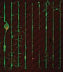
Patterning parylene on a silicon substrate and immersing it in horse serum enables the controlled growth of neurons and glia in specific configurations. |
A team of researchers from the University of Edinburgh (Scotland, UK; www.eng.ed.ac.uk) has developed a cell patterning technique that they believe is more simple, reliable, and easy to implement in most microfabrication processes than other cell patterning methods. In addition to enabling controlled growth patterns of neurons and glia on a silicon chip, the patterned substrates can be produced in bulk and even stored indefinitely for later use.
The technique employs photolithography methods to ultimately create cell patterns on a silicon substrate. To achieve this end result, researchers first grew a 200-nm-thick layer of silicon oxide on silicon wafers in a furnace at 950°C for 40 minutes. Next, they deposited a 100- to 200-nm-thick layer of the polymer parylene-C at room temperature onto the oxidized wafers and then patterned it using photolithography. Finally, the inert substrates were immersed and incubated in horse serum for a minimum of three hours in order to activate cell growth along the patterns.
Following the immersion and incubation period, the researchers discovered that neurons and glia adhered closely to the parylene pathways on the substrates that had been immersed in the serum. Cell growth on unpatterned control substrates, in contrast, was deemed arbitrary. The researchers have attributed the high compliance of cell growth within the designated serum-treated parylene patterns to the protein adhesion properties of
the polymer.
In light of this development, the scientists are currently in talks with pharmaceutical companies about the possibility of commercializing the technology. Silicon chips could reduce the need for animal testing in drug discovery and drug testing applications. The silicon technology may also have medical device applications—although that possibility is a more distant prospect, according to Alan Murray, professor of neural electronics and head of the School of Engineering at the university.
Because parylene is biocompatible, this patterning method could potentially be used in the fabrication of implants and prosthetics. In addition, patterned silicon chips could someday be used to replace damaged fibers or tissues. “That’s a long way off,” Murray notes, however. “We have only demonstrated patterning in vitro. If it does work in vivo, it would allow the potential for damaged nerve tissue to be encouraged to grow to electrodes on silicon.”
Copyright ©2009 Medical Product Manufacturing News
You May Also Like


