March 24, 2015
Graphene may not have replaced silicon in electronics yet, but researchers at three universities may have brought it a step closer.
Nancy Crotti
|
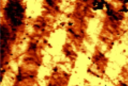
Check out the stripes in the above image, which show differences in electron density in graphene. (Photo courtesy of Lane Martin, through UC Berkeley) |
Graphene's one-atom thick lattice of carbon atoms allows for rapid movement of electrodesthrough its two-dimensional form. Now a team of researchers from the University of Pennsylvania; University of California, Berkeley; and University of Illinois at Urbana-Champaign has demonstrated a way to ease changing the polarity of a charge with an electric field, according to a publication by the UC Berkeley.
The researchers came up with a new way to change the number of electrons that reside in a given region within a piece of graphene. That has led them to a proof-of-principle in making the fundamental building blocks of semiconductor devices using the 2-D material, according to a statement by Penn.
Their method, recently published in the journal Nature Communications, enables this value to be tuned through the application of an electric field. That means that graphene circuit elements made in this way could one day be dynamically "rewired" without physically changing the device, according to the statement from Penn.
The number of free electrons contained in silicon can be easily changed by adding chemical impurities, creating either more positive or more negative charge carriers. The junctions between these carriers are the foundation of electronic devices. However, once added, the chemical impurities cannot be removed, the Penn statement said.
Doping graphene similarly would sacrifice some of its unique electrical properties, so the researchers placed a layer of graphene atop lithium niobate, a ferroelectric material whose surface can have either a positive or a negative charge. That's what can change the sign of the surface charges.
Applying an electric field pulse can change the sign of the surface charges, and graphene can take on the positive or negative electrons that the lithium discards.
"Because the lithium niobate domains can dictate the properties, different regions of graphene can take on different character depending on the nature of the domain underneath," Illinois researcher Moonsub Shim, said in the Penn statement. "That allows, as we have demonstrated, a simple means of creating a (positive-negative or p-n) junction or even an array of p-n junctions on a single flake of graphene. Such an ability should facilitate advances in graphene that might be analogous to what p-n junctions and complementary circuitry has done for the current state-of-the-art semiconductor electronics."
Future research will investigate the feasibility of designing dynamic semiconducting devices with this technique.
Graphene is not easy to make on a large scale. Based on research at Trinity College, Dublin,Thomas Swan & Co. Ltd (Consett, County Durham, UK) last year successfully scaled up a pilot manufacturing line able to produce up to a kilogram of high quality, few-layer graphene nanoplatelets.
In an unrelated development, a team of researchers from Nanyang Technological University (Singapore), Tsinghua University (Beijing), and Case Western Reserve University (CWRU; Cleveland, OH) last year developed a fiber-like, supercapacitor (battery) from graphene and carbon nanotubes that is flexible enough to be woven into clothing and has the highest energy density attained to date for a carbon-based supercapacitor. Supercapacitors have a lifespan about 10 times that of conventional rechargeable batteries.
Graphene is today's wonder material, but competition could be on the way. Another international research team announced earlier this month that it may have hit on a way to place crystalline lattices of pure electrons in the bottom of a silicon-encased quantum well, according to a report in Qmed's sister UBM publication, EE Times.
The resulting crystal electron "gas" would have electron mobility more than 200 times greater than graphene and more than 1700 times greater than crystalline silicon, professor Sergey Kravchenko at Northeastern University told EE Times. Such a material would fulfill theoretical predictions Nobel laureate Eugene Wigner made in 1934.
Refresh your medical device industry knowledge at BIOMEDevice Boston, May 6-7, 2015. |
Nancy Crotti is a contributor to Qmed and MPMN.
Like what you're reading? Subscribe to our daily e-newsletter.
About the Author(s)
You May Also Like


