Sign up for the QMED & MD+DI Daily newsletter.
Electromagnetic compatibility (EMC) is a major concern in medical electronics, considering that functional anomalies may be life threatening. In addition, design constraints, notably leakage current limitations, make the EMC design of medical electronic devices more difficult than their nonmedical counterparts.
14 Min Read
.svg?width=850&auto=webp&quality=95&format=jpg&disable=upscale "Exploring Systems EMC in Medical Devices")
With many devices, particularly small ones, the design approach is straightforward, using basic EMC design practices including shielding and filtering. But with more complex equipment, it may not be possible to protect the entire system, for one reason or another. For example, operator access may be needed during operation. Diagnostic equipment, injection systems, interventional lasers, and other devices may incorporate electric motors, lasers, high-power lamps, and power hardware for their functions.
Achieving EMC with complex systems may be not be easy, but following some basic guidelines at the front end of the design cycle eliminates many problems and minimizes the effect of those inevitable gremlins that show up downstream. The use of modest EMI (electromagnetic interference) control techniques throughout the system minimizes the need to take extraordinary steps at the last minute.
This article outlines the basic steps of systems EMC design for medical devices, but first some preliminary thoughts.
EMC Requirements: A Summary
EMC is pretty well covered by the regulatory requirements specified in IEC 60601, with modifications for special cases—technology always stays a step ahead of the regulators. Compliance with this standard is mandatory in much of the world, including the United States and Europe; most countries enforce it vigorously.
The standard covers both immunity to external interference and emissions from within the equipment, but the primary emphasis is on immunity, as it affects patient safety. Immunity requirements include external radiated electric and magnetic fields, conducted radio-frequency (RF) interference (RFI) and various power disturbances, and electrostatic discharge. (By the way, the term susceptibility is used instead of immunity in the military and automotive worlds—they are referring to the same issue.) The emission requirements limit energy emanating from the equipment to minimize interference to nearby electronic equipment, notably radio receiving equipment. This is usually not a safety issue, but there are exceptions.
The goal for all of the requirements is to ensure that the device will operate satisfactorily in its intended environment and degrade gracefully when the electromagnetic environment is worse than projected.
Basic EMC Concepts: Grounding and Shielding
Grounding and shielding form the core of EMC systems design.
|
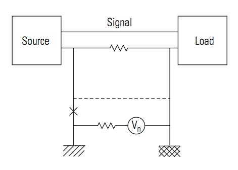
Figure 1. Effect of ground impedance. |
Grounding. The key issue in grounding is the impedance in the ground (or return path). Any time two or more circuits share a ground path, they also share voltage drop along the common path. The voltage generated by one circuit appears to the other circuit as an undesired signal. This is true wherever signal or ground currents flow, whether on the circuit board, interconnect cables, enclosure members, etc. Figure 1 shows the effect of ground impedance.
Single-point grounds are often cited as a solution to electromagnetic interference (EMI) problems, and they are very effective for controlling audio frequency noise. In Figure 1, the ground is broken at the “X” and moved to a single point, as indicated by the dashed line. However, single-point grounds are often not feasible. Worse, they don’t work at higher frequencies—path inductance and standing waves cause voltage drops along the way, and stray capacitance creates stray alternate paths. In these cases, the designer should look for low-impedance ground paths as the preferred way to control EMI.
The bottom line is, ground everything as often as possible. Don’t worry about ground loops. Once there is more than one ground, there is a multiple-point ground, and the only solution is to make impedance as low as possible. This task is best accomplished by using wide structural metal members, preferably sheet metal, and bolting them together at frequent intervals. If a metal chassis is not available, the only alternative is to ground through the cables, which is not a palatable choice—ground straps and wires are too inductive to be effective above audio frequencies.
Mating surfaces must be conductive and provided with a good contact area. Specifically, screw threads, hinges, latches, and bearings are unacceptable as ground connections.
In sum, multipoint grounds are needed for high frequencies and single-point grounds (or no grounds) are more appropriate for low-frequency analog circuits and motors.
|
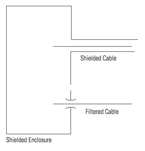
Figure 2. Basic shielded enclosure with shielded and filtered cables. |
Shielding. Figure 2 boils EMC shielding down to its basics. Any electronic device is at risk to external radiated interference, which can be contained through the use of a metallic shield. For the most part, this shield will contain radiated emissions from the device as well. The interference that enters or leaves the enclosure by conduction, through either the power or signal lines, need to be blocked by cable shielding or filtering. Thus, if a satisfactory shield can be implemented that either filters or shields the cables, this setup offers a solution to the regulatory issue. Of course the equipment still has to withstand internally generated interference.
Complete coverage of shielding and filtering would take up an entire book (and there are several good books available) and is beyond the scope of this article. However, a brief summary of the concepts is warranted because they are integral to the systems approach. Good shielding requires nearly complete closure—openings and seams must be minimized. In the authors’ experience, a good guideline to follow is that the longest dimension of the opening must be less than 1/20 of the wavelength of the highest threat frequency.
L = λ/20, where L is longest dimension of the opening and λ is wavelength, given by:
λ = 300/f. λ is measured in meters, f is in MHz.
The highest threat frequency will usually be the maximum RF immunity and emissions test frequency, usually 1 GHz. As an example, if there is a maximum threat frequency of 1 GHz, λ is 1/3 of a meter and maximum L = 1.5 cm. Of course, if the module can’t respond to a frequency that high, the closure requirements can be relaxed a bit.
Shielding can be achieved with any reasonably conductive material. Similarly, thickness of the material is also of little consequence—conductive coatings provide ample high-frequency shielding effectiveness. In almost all cases, the limitation is the openings; closing the seams will be the driving factor. The exception is shielding for low-frequency magnetic fields, especially 50–60 Hz, in which case thick, permeable materials are needed.
Wires penetrating the shield need to be shielded or filtered, depending on the application. As a rule, power lines and low-frequency signal lines are filtered and high-speed signal lines are shielded. In particular, patient-connected signal lines are essentially impossible to shield fully because the patient ends need to be exposed. The authors avoid transient suppressers, but they may be considered where permitted.
System Shielding
|
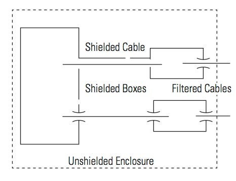
Figure 3. Unshielded enclosure with internal shielded boxes with internal shielded and filtered cables. |
Now that we have the basic shield in mind, note that the designer is free to select the shield boundaries, as long as those boundaries enclose the elements of interest, i.e., keep offending energy inside the shield and external energy outside of the shield. In the extreme case, there might be a single chip that is vulnerable to external radiated interference. Only the chip would need to be shielded, but there would still be concern about energy conducting into the pins. Or if the entire circuit board is a potential problem, some might shield the entire circuit board. Television works on this principle—the only circuit shielded is the TV tuner. Or, if we have a number of circuit boards, a shield might be used around the card cage.
But designers are not constrained to using a single shield; they can use as many as needed, as long as the shielding rules are followed for each module, and the wires penetrating the shield are either filtered or shielded. Figure 3 shows the principle: the shields have been moved inside to protect the critical areas, and shielded and filtered cables have been installed as needed to provide system protection.
Plan for EMI
Now that the basic grounding and shielding concepts are in mind, let’s turn to the initial design. The military world takes EMC seriously, usually requiring an EMI control plan (see DI-EMCS-80199B) to be prepared and submitted for review. Medical device manufacturers may not want to do this formally, but they should take the appropriate steps early in the design phase. The sooner EMI issues are addressed, the more design options there are. Consider the steps that follow.
1. Assess the Threat
If a manufacturer’s only concern is the regulatory issues (usually IEC 60601-1-2) and its equipment is covered by the requirements, this step is easy—all the thinking has been done for the company. But it is still appropriate to think beyond the regulations, by asking the following questions: What is the consequence of failure? Must the device be fully operable 100% of the time, or can it tolerate brief interruptions and, if so, for how long? These questions are pretty well covered by IEC 60601, but do perform a sanity check.
Is the equipment to be placed in an environment not adequately covered by IEC 60601? If it is to be operated in a vehicle, such as an emergency vehicle or aircraft, then the manufacturer might have to go beyond the regulations.
Are there any internal components that are especially noisy or sensitive? Here, the designer needs to consider not only the regulatory issues, but also the internal self-compatibility issues. Here are some quick guidelines.
Interference Sources. Continuous emitters include all clocks and associated data buses, switching power supplies and regulators, pulse-width modulation motor drives, electric motors, RF heaters, fluorescent lamps, and others. For the most part, these elements are generally only an issue with regards to emission limits, but RF heaters and diathermy may be energetic enough to create an internal interference situation.
Transient noise sources mostly originate from switching heavy loads, usually inductive loads such as motors and transformers. Starting loads tend to cause power sags and stopping loads tend to cause voltage spikes.
Interference Receptors. Although all electronics can be affected, given enough source energy, the authors find that analog input devices are much more vulnerable to RFI and digital devices are more vulnerable to transient events. Power electronics and electromechanical devices are usually the least vulnerable. But do note that the feedback path in voltage regulators are sensitive analog devices, and they are very sensitive to RFI. Even power and electrostatic discharge (ESD) transients can create a brief power sag, resulting in digital upset.
2. Partition the System
Most often, internal electrical or electronic modules are a subassembly, which might include a power supply, a microprocessor-based controller, patient connections, motors, actuators, and display and operator controls. Occasionally, it is feasible to combine two assemblies into one boundary, for example, the display and touch pad.
This setup is going to be just a part of the system design, as the location of these elements is probably going to be driven by considerations other than EMI. But where there are internal threats, EMI will have to be given its share of attention. As an example, physical separation of noisy sources and sensitive receptors is one of the best options—keep them as far apart as is feasible, including cables.
3. Decide on the Protection
Once the designer has decided on the key threats, the next step is deciding where to put the protection. Which modules need to be shielded, and which cables need to be filtered or shielded? Is the existing housing adequate or does it need to be shored up? If there are internal threats, potentially fighting with each other, then internal protection is needed. If all threats are external (either emissions or immunity), the protection boundaries can be placed where appropriate, as long as the protection lies between the affected circuits and the outside world. Where shielded cables are used, the shield must be circumferentially clamped to the connector shell and grounded at both ends.
Electromechanical devices such as ac or dc motors generally don’t need shielding, but may well require power filtering. Most electromechanical devices involve switching a substantial inductive load, so switching transients need to be contained, preferably as close to the load as possible. Usually, this containment is achieved by use of a resistor-capacitor filter or perhaps a diode snubber. Also note that motor drives (e.g., pulse-width modulation or variable frequency drivers) output substantial amounts of RF energy that will need to be contained, and power-cable shielding may well be a satisfactory choice for containment.
Microprocessor modules are the principal emitters, and they may also be vulnerable to RFI. These modules must be properly shielded. High-speed data cables often need to be shielded as well because filtering is usually not an option. Power-feed and low-frequency signals are generally filtered.
Visual displays are rarely shielded because shielding can degrade the image quality and brightness. Generally, the shield is placed behind the display, and the bezel is grounded at the perimeter to minimize antenna effects. Touch pads and operator controls need to be protected from ESD.
Patient isolation is one of the difficult areas. Full cable shielding is not feasible, and filtering is decidedly restricted—capacitance to enclosure ground is sharply limited. Basically, all protection needs to be referenced to the isolated area.
4. Design the Enclosure
Designing the enclosure requires the following.
|
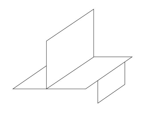
Figure 4. Complex ground plane. |
Design the Ground. This can’t be emphasized enough. Designers can use as much metal as they want (see Figure 4), but make sure that all the members follow the 5:1 rule mentioned previously, and that the mating surfaces are continuous or nearly continuous. Ideally, joints are welded or, as a second choice, secured with lots of screw fasteners.
Position the Modules Sensibly. Modules that interface with the outside world should be close to the enclosure boundary. Bolt all modules directly to ground. This guideline covers the module housing; the contents may be isolated from ground.
Ensure Low Impedance for Mating Surfaces. First, the mating surfaces need to be conductive. Painted surfaces and anodizing need to be masked at the mating surfaces. Conversion coatings can be used, but they need extra mating-surface area. Screw threads, hinges, latches, and shudder bearings are not satisfactory for low contact resistance. If these must be used, provide a ground strap to go around.
Such a setup poses a problem when mounting electronics on the door panel—there needs to be a good ground connection between the housing and the access door. At a minimum, route a ground strap between the housing and the door as well as running interconnections alongside the ground strap. Or better yet, run the cables through a cable shield and ground the cable shield at both ends.
5. Route Internal Cables
Once the ground is in place and the modules are bolted to the ground, the cables need to be routed. First and foremost, put the cables under control drawing. Internal cables should be routed adjacent to ground to minimize loop areas and, hence, antenna effects. Space the cables to minimize crosstalk between high-energy cables near sensitive receiving circuits. Where they must cross, make a perpendicular crossing.
6. Ground Shielded Housings
Metal housings (motors, power supplies, card cages, etc.) need to be grounded to each other and to the ground system previously described. Floating or poorly grounded metallic members do no good and may even cause problems.
7. Conduct Preliminary Testing
Waiting until the last minute to get test data guarantees schedule slippage and cost overruns. Get preliminary test data as early as possible so that corrective action can be taken early in the game. Everything doesn’t have to be working in order to obtain useful test information—you don’t need to do full testing, and the test need not be highly calibrated. The sooner the testing is done, the more options there are for fixing problems.
Conclusion
EMC requires planning and it won’t happen by accident. Follow the military guidelines for planning and executing an EMC program, at least informally. Don’t use the excuse that there isn’t time. As one of Murphy’s laws says, “There is never time to do it right, but there is always time to do it over.”
Most EMC problems are identifiable. With a little planning, major problems and many minor problems can be avoided. Most notably, low impedance grounding is mandatory. There will always be something you missed, but if you have done your homework, the problem should be fixable without major redesign.
Bibliography
DI-EMCS-80199B, “Electromagnetic Interference Control Procedures (EMCP),” 1990.
IEC 60601-1-2, “Medical Electrical Equipment—Part 1–2: General Requirements for Basic Safety and Essential Performance—Collateral Standard: Electromagnetic Compatibility—Requirements and Tests” (Brussels: International Electrotechnical Commission, 2005).
William D. Kimmel, PE, and Daryl D. Gerke, PE, are partners in Kimmel Gerke Associates Ltd. (South St. Paul, MN, and Mesa, AZ).
About the Author(s)
You May Also Like
Editors' Choice

Sponsored Content
May 22, 2024